Key Points of AI Hardware PCB Design
- Staff Desk
- Jan 22
- 7 min read


As artificial intelligence continues to deeply penetrate multiple scenarios—such as edge computing, AI cameras, AI robots, and AI servers—AI hardware is rapidly evolving toward higher computing power, greater integration, and stronger reliability. As the core carrier of AI hardware, PCB design directly determines the performance of AI chips, the stability of device operation, and even the product’s market competitiveness.
Unlike traditional consumer electronics PCBs, AI hardware—especially in high-performance computing scenarios—places extremely stringent requirements on electrical performance, thermal management, and signal integrity. These requirements are often the most significant bottlenecks encountered during the R&D process.
This article focuses on the four core key points of AI hardware PCB design, breaking down the main design challenges and optimization strategies. It aims to provide practical reference for AI hardware developers, helping to overcome design difficulties and improve product competitiveness. This is also the core experience summary of our work in the AI hardware PCB design field, where we have delivered customized solutions to numerous AI companies.

High-Performance AI Modules
Power Delivery
High-performance AI modules are extremely sensitive to power supply ripple and noise. Even minor fluctuations can lead to reduced compute performance, data errors, or even chip damage. Therefore, it is crucial to optimize the power distribution network (PDN). This typically includes:
l Using 2 oz or thicker copper for power traces
l Properly sizing trace width based on current to keep current density below 15 A/mm², reducing heat generation and voltage drop
l Implementing multi-layer power planes, paired with high-precision filtering capacitors, to keep supply ripple within ±2%
l Ensuring stable high-current output to meet transient power demands of AI chips
For compact AI edge devices with limited PCB space, multi-rail power delivery can be achieved using integrated power modules, which simplify routing while improving reliability.
Thermal Management
Thermal design is the “lifeline” of high-performance AI PCBs. If the heat generated by high power consumption cannot be dissipated effectively, it can accelerate PCB substrate aging, cause solder joint failure, and trigger thermal throttling, significantly reducing mean time between failures (MTBF).
In practice, a composite thermal structure such as copper base + embedded heat pipe can raise PCB thermal conductivity to over 5 W/(m·K). Coupled with a dense array of thermal vias beneath the AI chip, heat can be rapidly transferred to heatsinks on the PCB’s backside. For high heat-flux devices like AI servers and training cards, a hybrid FR-4 + aluminum substrate can further reduce hotspot temperatures, ensuring junction temperature stays below 85°C.
Thermal simulation tools can model heat transfer paths under different layouts and automatically adjust component placement and routing. This approach can reduce hotspot temperatures by 10–15°C, greatly improving cooling efficiency.
EMI Control
EMI control is essential for both compliance and stable operation. High-speed signal transmission and large current switching in AI modules easily generate electromagnetic radiation, and are also susceptible to external interference, which can degrade algorithm accuracy.
Design practices should follow a partitioning and isolation strategy: separate power areas, high-frequency signal areas, and analog sections; use ground isolation strips and shielding enclosures to reduce cross-region interference. During routing, minimize the length of high-frequency traces and high-current lines, avoid parallel routing, and reduce electromagnetic coupling. Selecting low-loss, high-stability PCB materials also helps suppress EMI, ensuring the AI hardware meets industry electromagnetic compatibility standards.
At the same time, working with a reputable manufacturer that provides excellent PCB fabrication services is critical to ensuring consistent material quality, precise impedance control, and reliable EMI performance
High-Speed Signal Integrity

DDR (DDR4/DDR5) Signal Integrity
DDR memory speeds have surpassed 4800 Mbps, requiring extremely strict timing alignment and impedance control. Key design requirements include:
l Fly-by topology for address/command routing, with automated pin ordering and timing adjustments to meet CK-to-DQS skew constraints
l Tight length matching within each signal group, keeping length differences below 5 mil to prevent timing mismatches
l Precise impedance control: maintain DDR trace impedance at 50 Ω ± 3%
l Use series termination resistors to reduce signal reflections and crosstalk, ensuring memory read/write error rates below 10^-9
PCIe Interface (PCIe 6.0)
PCIe is the core high-speed interconnect for AI hardware. With PCIe 6.0 reaching 64 GB/s, the margin for signal attenuation and crosstalk is extremely small. This interface is critical for multi-GPU interconnects, AI accelerator cards, and motherboard communication.
Design recommendations include:
l Use high-frequency, low-loss substrates (e.g., Rogers RO4835, Shengyi S1000-2) with tanδ ≤ 0.004 @ 10 GHz, keeping attenuation below 0.8 dB/in for 64 GB/s signals—significantly better than standard FR-4
l Differential pair routing with strict control of trace width and spacing to maintain 85 Ω ± 3% differential impedance
l Provide adequate isolation spacing and use ground isolation strips to reduce crosstalk
l Use tools like Polar SI9000 for routing parameter calculations, and calibrate each board with an impedance analyzer during production to ensure high signal integrity. Target performance includes: eye height ≥ 0.9 V, jitter ≤ 80 ps, and bit error rate below 10^-12
High-Speed Ethernet and USB4
High-speed Ethernet (such as 10G/25G) and USB4 are also key data transmission interfaces for AI edge devices and AI cameras. The main challenges are signal attenuation and crosstalk.
Key practices include:
l Use ceramic-filled high-frequency substrates to control signal loss at 10 GHz to around 0.25 dB/in, reducing loss by about 45% compared to traditional FR-4
l Implement precision impedance control and low-roughness trace processes. For example, laser etching can achieve edge roughness Ra < 0.5 μm, optimizing reflection coefficient (S11) to -30 dB, ensuring distortion-free transmission
l Plan routing carefully to avoid crossing split power planes, which can introduce interference and degrade signal integrity
Advanced Reading: Strategies to Reduce Signal Integrity Issues in PCB Design
BGA Reliability for AI SoCs/ FPGAs
Pad Design and Routing Optimization
The primary challenge in BGA PCB design is optimizing pad geometry and routing. Pad sizes must strictly match the chip’s pin specifications—pads that are too large or too small can lead to poor solder joints and opens. Due to high pin density, routing requires blind/buried vias and microvias, especially HDI (High-Density Interconnect) 3rd-order blind/buried via technology. This allows 0.1 mm microvia drilling and routing densities up to 200 traces/cm², which is about 50% higher than traditional PCB processes, effectively solving routing congestion for high pin-count BGAs.
For example, under a 0.8 mm × 0.8 mm BGA package, AI-driven routing algorithms can plan 0.08 mm trace-width paths, accommodating 20% more traces than manual routing, significantly improving routing efficiency and density.
Thermal and Mechanical Reliability
BGA heat is primarily transferred to the PCB through the solder balls. If heat dissipation is inadequate, internal temperatures rise, which affects chip performance and solder joint reliability. Additionally, AI hardware often operates under vibration; if solder joints lack mechanical strength, they may crack or detach.
To address this, designers should:
l Place thermal via arrays under the BGA to enhance heat conduction
l Use PCB substrates with high Tg (≥170°C) to improve thermal resistance and reduce soldering stress
l Optimize copper distribution and increase copper area around solder joints to strengthen mechanical robustness and prevent vibration-induced failures
Signal Integrity and Manufacturing Quality
Signal integrity for BGA packages also requires careful attention. Narrow pin pitches increase the risk of crosstalk. High-speed and low-speed signals, as well as analog and digital signals, should be routed separately to avoid interference. Power and ground pin placement should be planned to enable effective decoupling. Placing sufficient decoupling capacitors around the BGA reduces power noise and ensures stable signal transmission.
In production, using LDI (Laser Direct Imaging) with positioning accuracy of ±2 μm, along with AOI + AXI dual inspection, can keep short/open defects below 0.03%, ensuring reliable BGA soldering.
Stack-Up Strategy Optimization
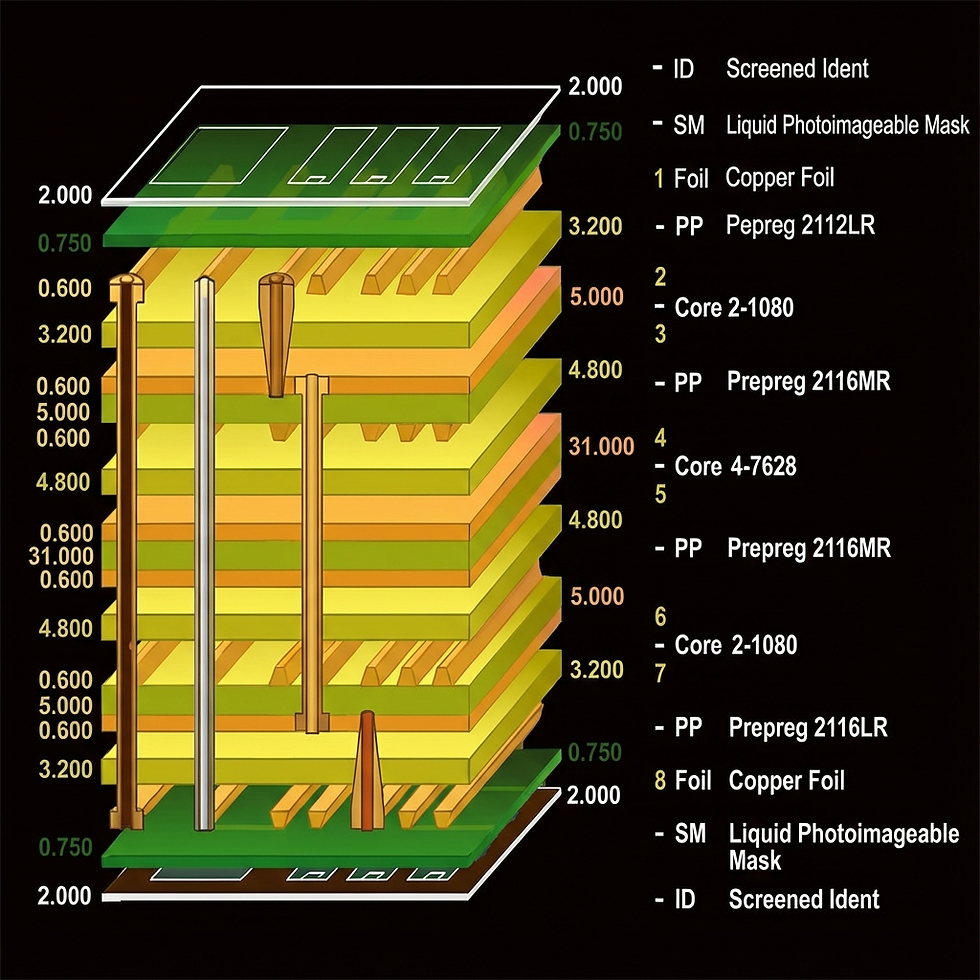
2+N+2 Stack-Up: The Preferred Choice for High-Performance AI Systems
The 2+N+2 stack-up is the preferred solution for high-performance AI hardware, especially in AI servers and training cards. The structure consists of:
l Top signal layer
l N internal layers (power, ground, and signal layers)
l Bottom signal layer
The number of internal layers (N) can be flexibly configured according to design needs. Power and ground layers are implemented as continuous planes, which helps reduce power noise, improve signal integrity, and enhance thermal dissipation.
For example, an AI server PCB using a 2+8+2 stack-up can separate multiple power and ground planes to support multiple GPUs and memory modules. At the same time, a continuous ground plane effectively suppresses EMI and improves system stability.
HDI PCBs: Ideal for Compact, High-Integration AI Devices
HDI PCBs are particularly suitable for compact, high-integration AI devices such as edge computing hardware, AI cameras, and AI robots. These devices have limited PCB space but require many components and high-speed interfaces. HDI technology uses microvias and blind/buried vias to achieve high routing density within limited space, reducing board area while shortening signal paths and minimizing latency and crosstalk.
For instance, an AI accelerator card using HDI 3rd-order blind/buried vias successfully integrates eight high-performance chips, increasing computing density to 20 TOPS/cm². The PCB volume is reduced by 40% compared to traditional designs, making it a perfect fit for compact AI hardware.
Multilayer Board Design: Layer Planning and Functional Partitioning
The core of multilayer stack-up design lies in layer planning and functional partitioning. Designers should define the purpose of each layer based on the AI system’s functional requirements:
l Place power and ground layers adjacent to reduce power noise through capacitive coupling
l Place high-speed signal layers adjacent to ground layers to reduce radiation and interference
l Separate analog and digital layers to avoid digital noise affecting analog circuits
Additionally, stack-up thickness and copper weight should be optimized. AI PCBs typically use 1.6 mm to 2.0 mm board thickness and 1 oz to 3 oz copper. Core power regions may use 3 oz copper to enhance heat dissipation and current-carrying capability.
Moreover, by leveraging AI algorithms to automatically match layer count, trace width, spacing, and other parameters, designers can generate an optimal stack-up quickly—transforming the traditional “iterative revisions” into “one-time success,” and reducing development cycles by 30%–50%.
Conclusion
AI hardware PCB design is a high-stakes task where layout decisions directly affect performance and reliability. If your product targets high compute, high integration, or high-speed interfaces, the PCB must be engineered with the right expertise and manufacturing support.
For high-end AI hardware, choosing a PCB manufacturer with advanced capabilities is not optional—it’s essential. The best outcomes typically come from partners who can provide consistent quality, tight tolerances, and reliable production processes, supported by proper certifications and quality systems (such as ISO 9001 and IPC compliance).
If you are building AI servers, AI edge devices, or AI vision systems, selecting the right EMS PCB manufacturer can make the difference between a prototype and a product that scales.


Comments